PCB Design
We were able to convert a concept into a circuit design with all the components figured out. But now, it’s time to dive a bit deeper into finding the footprints for each of these components and try to build a PCB for this circuit!
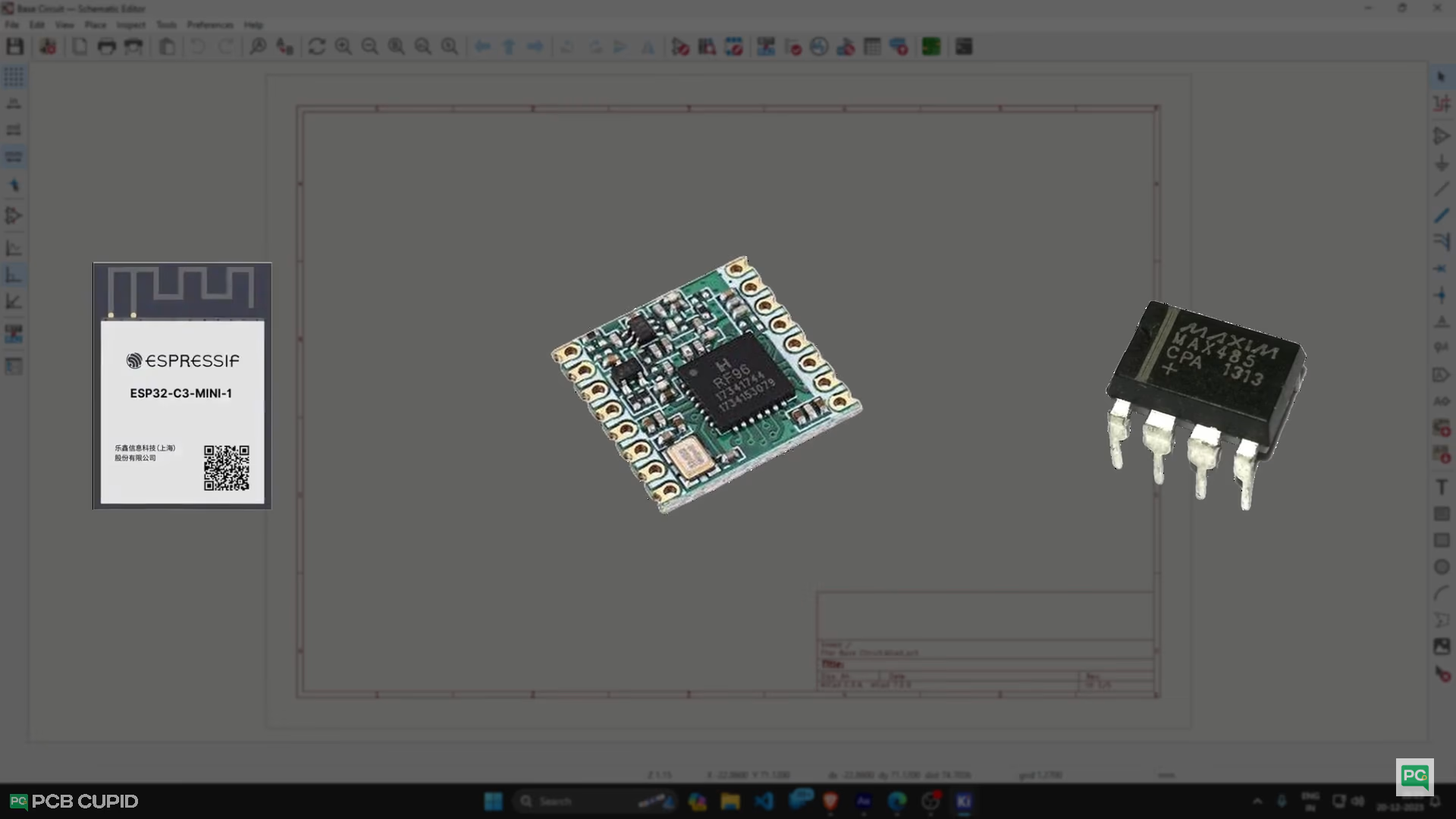
I have already made a dedicated video explaining what footprint is and how to assign footprint to components. So, if you are new to PCB, I would strongly suggest you watch those videos before moving further with this.
Choosing the right footprint isn't just random because it involves more than just engineering; we also need to carefully assess the finances, labour and supply chain before even starting the design process!
Footprint Selection
That’s the reason I have a list of Footprint Selection checkboxes that I use to select the right component and footprint for my PCB.
And these are the major points I consider while selecting the component or the footprint: type, Size, Usability, Availability, Long term support and Cost.
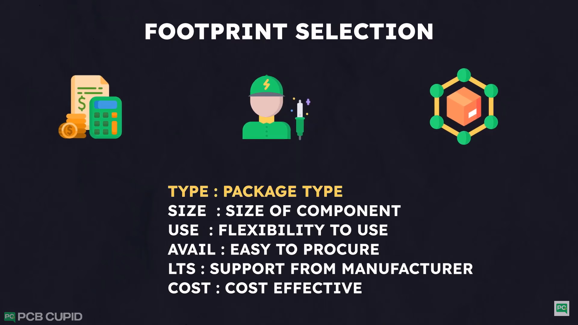
- Cost: Cheaper components and footprints translate to a cheaper overall product.
- Size: Smaller footprints save space, but might be harder to assemble.
- Availability: Can we easily source the components with the chosen footprints?
- Longevity: Will these components and footprints be supported in the future?
- Usability: How easy is it to use the finished PCB after assembly?
PCB Design
Since we have the component and footprint ready, let’s dive into the PCB design. First, I did all the basic necessities, like filling up the design rules, assigning net classes and setting up track widths.
With all the basic setup done, I will make sure to follow all the basic rules of PCB design while designing.
Here, I will make different sections on the PCB to keep things very simple, which also helps in reducing interference and avoiding noise. Especially when dealing with the RF circuit and SMPS circuit.
Then follow the recommended design layout and place the components in there respective sections. You can sometimes find this recommended layout in the datasheet, or you can take reference from a reliable pre-existing product or circuit.
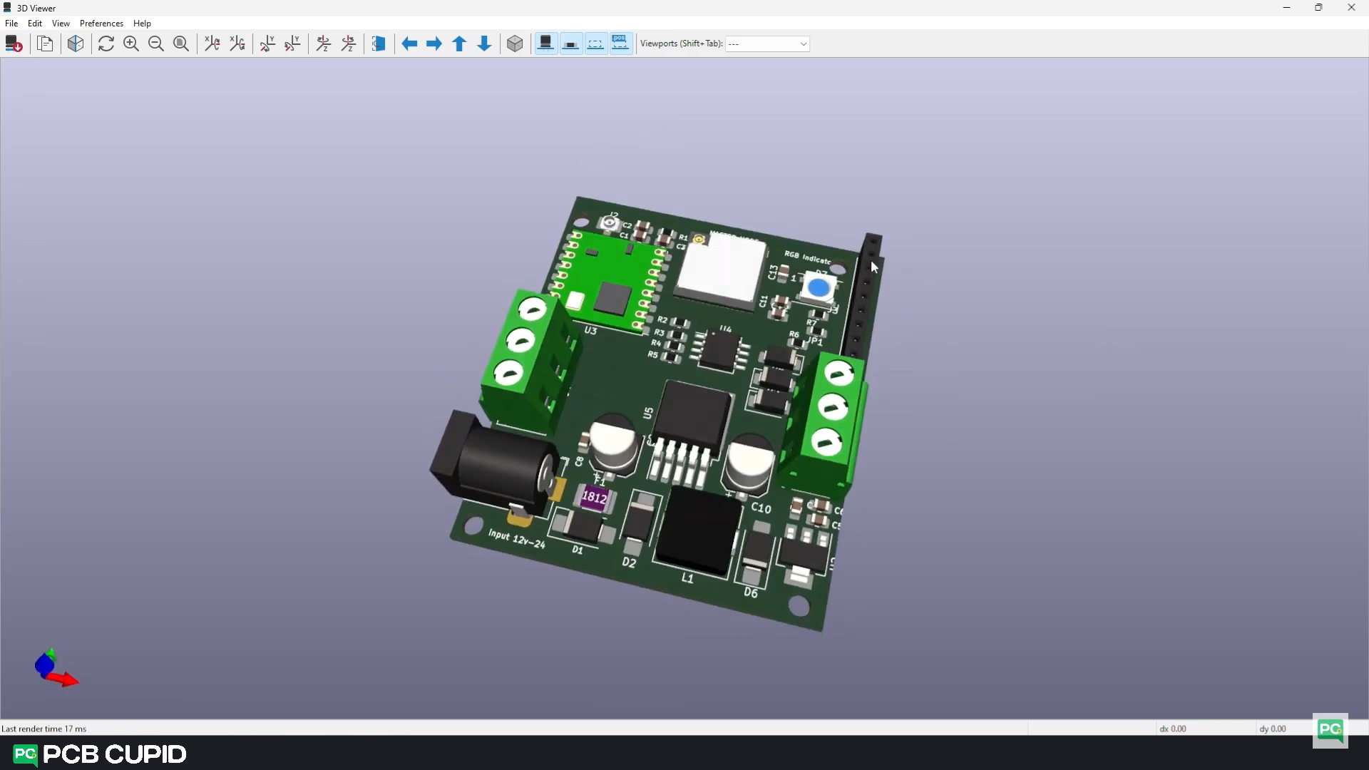
In this stage, I also make sure I get all the 3D models into the PCB layout so I can place the components, not only based on the footprint but also based on accessibility and clearance.
Once we have the PCB layout ready, we can start with routing!
PCB Routing
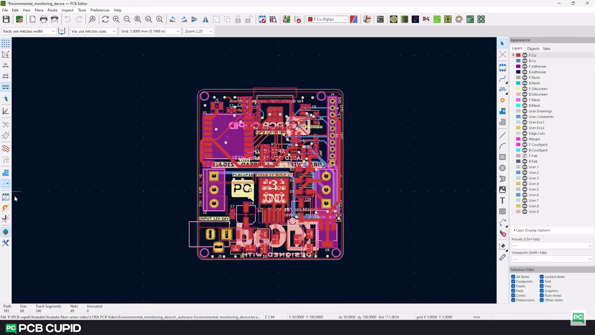
We can start with auto routing and then refine the output, but the auto router will struggle in the power section and RF section, so I will manually route the whole PCB.
Once the routing is done, do a thorough check on the circuit as well as on the PCB to make sure everything is proper and generate the gerber file.